 | –≠–ª–µ–∫—Ç—Ä–æ–Ω–Ω—ã–π –∫–æ–º–ø–æ–Ω–µ–Ω—Ç: 2N6052 | –°–∫–∞—á–∞—Ç—å:  PDF PDF  ZIP ZIP |

Darlington Complementary
Silicon Power Transistors
. . . designed for general≠purpose amplifier and low frequency
switching applications.
∑
High DC Current Gain --
h
FE
= 3500 (Typ) @ I
C
= 5.0 Adc
∑
Collector≠Emitter Sustaining Voltage -- @ 100 mA
V
CEO(sus)
=
80 Vdc (Min) -- 2N6058
100 Vdc (Min) -- 2N6052, 2N6059
∑
Monolithic Construction with Built≠In Base≠Emitter Shunt Resistors
ŒŒŒŒŒŒŒŒŒŒŒŒŒŒŒŒŒŒŒŒŒŒŒ
ŒŒŒŒŒŒŒŒŒŒŒŒŒŒŒŒŒŒŒŒŒŒŒ
MAXIMUM RATINGS (1)
ŒŒŒŒŒŒŒŒŒŒŒŒ
Œ
ŒŒŒŒŒŒŒŒŒŒ
Œ
ŒŒŒŒŒŒŒŒŒŒŒŒ
Rating
ŒŒŒŒ
Œ
ŒŒ
Œ
ŒŒŒŒ
Symbol
ŒŒŒŒ
Œ
ŒŒ
Œ
ŒŒŒŒ
2N6058
ŒŒŒŒ
Œ
ŒŒ
Œ
ŒŒŒŒ
2N6052
2N6059
ŒŒŒ
Œ
Œ
Œ
ŒŒŒ
Unit
ŒŒŒŒŒŒŒŒŒŒŒŒ
ŒŒŒŒŒŒŒŒŒŒŒŒ
Collector≠Emitter Voltage
ŒŒŒŒ
ŒŒŒŒ
V
CEO
ŒŒŒŒ
ŒŒŒŒ
80
ŒŒŒŒ
ŒŒŒŒ
100
ŒŒŒ
ŒŒŒ
Vdc
ŒŒŒŒŒŒŒŒŒŒŒŒ
ŒŒŒŒŒŒŒŒŒŒŒŒ
Collector≠Base Voltage
ŒŒŒŒ
ŒŒŒŒ
V
CB
ŒŒŒŒ
ŒŒŒŒ
80
ŒŒŒŒ
ŒŒŒŒ
100
ŒŒŒ
ŒŒŒ
Vdc
ŒŒŒŒŒŒŒŒŒŒŒŒ
ŒŒŒŒŒŒŒŒŒŒŒŒ
Emitter≠Base voltage
ŒŒŒŒ
ŒŒŒŒ
V
EB
ŒŒŒŒŒŒŒ
ŒŒŒŒŒŒŒ
5.0
ŒŒŒ
ŒŒŒ
Vdc
ŒŒŒŒŒŒŒŒŒŒŒŒ
Œ
ŒŒŒŒŒŒŒŒŒŒ
Œ
ŒŒŒŒŒŒŒŒŒŒŒŒ
Collector Current -- Continuous
Peak
ŒŒŒŒ
Œ
ŒŒ
Œ
ŒŒŒŒ
I
C
ŒŒŒŒŒŒŒ
Œ
ŒŒŒŒŒ
Œ
ŒŒŒŒŒŒŒ
12
20
ŒŒŒ
Œ
Œ
Œ
ŒŒŒ
Adc
ŒŒŒŒŒŒŒŒŒŒŒŒ
ŒŒŒŒŒŒŒŒŒŒŒŒ
Base Current
ŒŒŒŒ
ŒŒŒŒ
I
B
ŒŒŒŒŒŒŒ
ŒŒŒŒŒŒŒ
0.2
ŒŒŒ
ŒŒŒ
Adc
ŒŒŒŒŒŒŒŒŒŒŒŒ
Œ
ŒŒŒŒŒŒŒŒŒŒ
Œ
ŒŒŒŒŒŒŒŒŒŒŒŒ
Total Device Dissipation
@T
C
= 25
_
C
Derate above 25
_
C
ŒŒŒŒ
Œ
ŒŒ
Œ
ŒŒŒŒ
P
D
ŒŒŒŒŒŒŒ
Œ
ŒŒŒŒŒ
Œ
ŒŒŒŒŒŒŒ
150
0.857
ŒŒŒ
Œ
Œ
Œ
ŒŒŒ
Watts
W/
_
C
ŒŒŒŒŒŒŒŒŒŒŒŒ
Œ
ŒŒŒŒŒŒŒŒŒŒ
Œ
ŒŒŒŒŒŒŒŒŒŒŒŒ
Operating and Storage Junction
Temperature Range
ŒŒŒŒ
Œ
ŒŒ
Œ
ŒŒŒŒ
T
J
, T
stg
ŒŒŒŒŒŒŒ
Œ
ŒŒŒŒŒ
Œ
ŒŒŒŒŒŒŒ
≠65 to +200
_
C
ŒŒŒ
Œ
Œ
Œ
ŒŒŒ
_
C
ŒŒŒŒŒŒŒŒŒŒŒŒŒŒŒŒŒŒŒŒŒŒŒ
ŒŒŒŒŒŒŒŒŒŒŒŒŒŒŒŒŒŒŒŒŒŒŒ
THERMAL CHARACTERISTICS
ŒŒŒŒŒŒŒŒŒŒŒŒ
ŒŒŒŒŒŒŒŒŒŒŒŒ
Characteristic
ŒŒŒŒŒ
ŒŒŒŒŒ
Symbol
ŒŒŒŒŒŒ
ŒŒŒŒŒŒ
Rating
ŒŒŒ
ŒŒŒ
Unit
ŒŒŒŒŒŒŒŒŒŒŒŒ
ŒŒŒŒŒŒŒŒŒŒŒŒ
Thermal Resistance, Junction to Case
ŒŒŒŒŒ
ŒŒŒŒŒ
R
JC
ŒŒŒŒŒŒ
ŒŒŒŒŒŒ
1.17
ŒŒŒ
ŒŒŒ
_
C/W
(1) Indicates JEDEC Registered Data.
160
0
0
25
50
75
100
125
150
200
Figure 1. Power Derating
T
C
, CASE TEMPERATURE (
∞
C)
P D
, POWER DISSIP
A
TION (W
A
TTS)
120
100
140
175
80
40
20
60
Preferred devices are ON Semiconductor recommended choices for future use and best overall value.
ON Semiconductort
©
Semiconductor Components Industries, LLC, 2001
March, 2001 ≠ Rev. 2
1
Publication Order Number:
2N6052/D
2N6052
2N6058
2N6059
*ON Semiconductor Preferred Device
DARLINGTON
12 AMPERE
COMPLEMENTARY
SILICON
POWER TRANSISTORS
80≠100 VOLTS
150 WATTS
*
*
CASE 1≠07
TO≠204AA
(TO≠3)
PNP
NPN

2N6052
http://onsemi.com
2
ŒŒŒŒŒŒŒŒŒŒŒŒŒŒŒŒŒŒŒŒŒŒŒŒŒŒŒŒŒŒŒŒŒ
ŒŒŒŒŒŒŒŒŒŒŒŒŒŒŒŒŒŒŒŒŒŒŒŒŒŒŒŒŒŒŒŒŒ
*ELECTRICAL CHARACTERISTICS
(T
C
= 25
_
C unless otherwise noted)
ŒŒŒŒŒŒŒŒŒŒŒŒŒŒŒŒŒŒŒŒŒŒ
ŒŒŒŒŒŒŒŒŒŒŒŒŒŒŒŒŒŒŒŒŒŒ
Characteristic
ŒŒŒŒŒ
ŒŒŒŒŒ
Symbol
ŒŒŒ
ŒŒŒ
Min
ŒŒŒŒ
ŒŒŒŒ
Max
ŒŒŒ
ŒŒŒ
Unit
ŒŒŒŒŒŒŒŒŒŒŒŒŒŒŒŒŒŒŒŒŒŒŒŒŒŒŒŒŒŒŒŒŒ
ŒŒŒŒŒŒŒŒŒŒŒŒŒŒŒŒŒŒŒŒŒŒŒŒŒŒŒŒŒŒŒŒŒ
OFF CHARACTERISTICS
ŒŒŒŒŒŒŒŒŒŒŒŒŒŒŒŒŒŒŒŒŒŒ
Œ
ŒŒŒŒŒŒŒŒŒŒŒŒŒŒŒŒŒŒŒŒ
Œ
ŒŒŒŒŒŒŒŒŒŒŒŒŒŒŒŒŒŒŒŒŒŒ
Collector≠Emitter Sustaining Voltage (2)
(I
C
= 100 mAdc, I
B
= 0)
2N6058
2N6052, 2N6059
ŒŒŒŒŒ
Œ
ŒŒŒ
Œ
ŒŒŒŒŒ
V
CEO(sus)
ŒŒŒ
Œ
Œ
Œ
ŒŒŒ
80
100
ŒŒŒŒ
Œ
ŒŒ
Œ
ŒŒŒŒ
--
--
ŒŒŒ
Œ
Œ
Œ
ŒŒŒ
Vdc
ŒŒŒŒŒŒŒŒŒŒŒŒŒŒŒŒŒŒŒŒŒŒ
Œ
ŒŒŒŒŒŒŒŒŒŒŒŒŒŒŒŒŒŒŒŒ
Œ
Œ
ŒŒŒŒŒŒŒŒŒŒŒŒŒŒŒŒŒŒŒŒ
Œ
ŒŒŒŒŒŒŒŒŒŒŒŒŒŒŒŒŒŒŒŒŒŒ
Collector Cutoff Current
(V
CE
= 40 Vdc, I
B
= 0)
2N6058
(V
CE
= 50 Vdc, I
B
= 0)
2N6052, 2N6059
ŒŒŒŒŒ
Œ
ŒŒŒ
Œ
Œ
ŒŒŒ
Œ
ŒŒŒŒŒ
I
CEO
ŒŒŒ
Œ
Œ
Œ
Œ
Œ
Œ
ŒŒŒ
--
--
ŒŒŒŒ
Œ
ŒŒ
Œ
Œ
ŒŒ
Œ
ŒŒŒŒ
1.0
1.0
ŒŒŒ
Œ
Œ
Œ
Œ
Œ
Œ
ŒŒŒ
mAdc
ŒŒŒŒŒŒŒŒŒŒŒŒŒŒŒŒŒŒŒŒŒŒ
Œ
ŒŒŒŒŒŒŒŒŒŒŒŒŒŒŒŒŒŒŒŒ
Œ
ŒŒŒŒŒŒŒŒŒŒŒŒŒŒŒŒŒŒŒŒŒŒ
Collector Cutoff Current
(V
CE
= Rated V
CEO
, V
BE(off)
= 1.5 Vdc)
(V
CE
= Rated V
CEO
, V
BE(off)
= 1.5 Vdc, T
C
= 150
_
C)
ŒŒŒŒŒ
Œ
ŒŒŒ
Œ
ŒŒŒŒŒ
I
CEX
ŒŒŒ
Œ
Œ
Œ
ŒŒŒ
--
ŒŒŒŒ
Œ
ŒŒ
Œ
ŒŒŒŒ
0.5
5.0
ŒŒŒ
Œ
Œ
Œ
ŒŒŒ
mAdc
ŒŒŒŒŒŒŒŒŒŒŒŒŒŒŒŒŒŒŒŒŒŒ
Œ
ŒŒŒŒŒŒŒŒŒŒŒŒŒŒŒŒŒŒŒŒ
Œ
ŒŒŒŒŒŒŒŒŒŒŒŒŒŒŒŒŒŒŒŒŒŒ
Emitter Cutoff Current
(V
BE
= 5.0 Vdc, I
C
= 0)
ŒŒŒŒŒ
Œ
ŒŒŒ
Œ
ŒŒŒŒŒ
I
EBO
ŒŒŒ
Œ
Œ
Œ
ŒŒŒ
--
ŒŒŒŒ
Œ
ŒŒ
Œ
ŒŒŒŒ
2.0
ŒŒŒ
Œ
Œ
Œ
ŒŒŒ
mAdc
ŒŒŒŒŒŒŒŒŒŒŒŒŒŒŒŒŒŒŒŒŒŒŒŒŒŒŒŒŒŒŒŒŒ
ŒŒŒŒŒŒŒŒŒŒŒŒŒŒŒŒŒŒŒŒŒŒŒŒŒŒŒŒŒŒŒŒŒ
ON CHARACTERISTICS (2)
ŒŒŒŒŒŒŒŒŒŒŒŒŒŒŒŒŒŒŒŒŒŒ
Œ
ŒŒŒŒŒŒŒŒŒŒŒŒŒŒŒŒŒŒŒŒ
Œ
ŒŒŒŒŒŒŒŒŒŒŒŒŒŒŒŒŒŒŒŒŒŒ
DC Current Gain
(I
C
= 6.0 Adc, V
CE
= 3.0 Vdc)
(I
C
= 12 Adc, V
CE
= 3.0 Vdc)
ŒŒŒŒŒ
Œ
ŒŒŒ
Œ
ŒŒŒŒŒ
h
FE
ŒŒŒ
Œ
Œ
Œ
ŒŒŒ
750
100
ŒŒŒŒ
Œ
ŒŒ
Œ
ŒŒŒŒ
18,000
--
ŒŒŒ
Œ
Œ
Œ
ŒŒŒ
--
ŒŒŒŒŒŒŒŒŒŒŒŒŒŒŒŒŒŒŒŒŒŒ
Œ
ŒŒŒŒŒŒŒŒŒŒŒŒŒŒŒŒŒŒŒŒ
Œ
Œ
ŒŒŒŒŒŒŒŒŒŒŒŒŒŒŒŒŒŒŒŒ
Œ
ŒŒŒŒŒŒŒŒŒŒŒŒŒŒŒŒŒŒŒŒŒŒ
Collector≠Emitter Saturation Voltage
(I
C
= 6.0 Adc, I
B
= 24 mAdc)
(I
C
= 12 Adc, I
B
= 120 mAdc)
ŒŒŒŒŒ
Œ
ŒŒŒ
Œ
Œ
ŒŒŒ
Œ
ŒŒŒŒŒ
V
CE(sat)
ŒŒŒ
Œ
Œ
Œ
Œ
Œ
Œ
ŒŒŒ
--
--
ŒŒŒŒ
Œ
ŒŒ
Œ
Œ
ŒŒ
Œ
ŒŒŒŒ
2.0
3.0
ŒŒŒ
Œ
Œ
Œ
Œ
Œ
Œ
ŒŒŒ
Vdc
ŒŒŒŒŒŒŒŒŒŒŒŒŒŒŒŒŒŒŒŒŒŒ
ŒŒŒŒŒŒŒŒŒŒŒŒŒŒŒŒŒŒŒŒŒŒ
Base≠Emitter Saturation Voltage
(I
C
= 12 Adc, I
B
= 120 mAdc)
ŒŒŒŒŒ
ŒŒŒŒŒ
V
BE(sat)
ŒŒŒ
ŒŒŒ
--
ŒŒŒŒ
ŒŒŒŒ
4.0
ŒŒŒ
ŒŒŒ
Vdc
ŒŒŒŒŒŒŒŒŒŒŒŒŒŒŒŒŒŒŒŒŒŒ
Œ
ŒŒŒŒŒŒŒŒŒŒŒŒŒŒŒŒŒŒŒŒ
Œ
ŒŒŒŒŒŒŒŒŒŒŒŒŒŒŒŒŒŒŒŒŒŒ
Base≠Emitter On Voltage
(I
C
= 6.0 Adc, V
CE
= 3.0 Vdc)
ŒŒŒŒŒ
Œ
ŒŒŒ
Œ
ŒŒŒŒŒ
V
BE(on)
ŒŒŒ
Œ
Œ
Œ
ŒŒŒ
--
ŒŒŒŒ
Œ
ŒŒ
Œ
ŒŒŒŒ
2.8
ŒŒŒ
Œ
Œ
Œ
ŒŒŒ
Vdc
ŒŒŒŒŒŒŒŒŒŒŒŒŒŒŒŒŒŒŒŒŒŒŒŒŒŒŒŒŒŒŒŒŒ
ŒŒŒŒŒŒŒŒŒŒŒŒŒŒŒŒŒŒŒŒŒŒŒŒŒŒŒŒŒŒŒŒŒ
DYNAMIC CHARACTERISTICS
ŒŒŒŒŒŒŒŒŒŒŒŒŒŒŒŒŒŒŒŒŒŒ
Œ
ŒŒŒŒŒŒŒŒŒŒŒŒŒŒŒŒŒŒŒŒ
Œ
ŒŒŒŒŒŒŒŒŒŒŒŒŒŒŒŒŒŒŒŒŒŒ
Magnitude of Common Emitter Small≠Signal Short Circuit Forward
Current Transfer Ratio
(I
C
= 5.0 Adc, V
CE
= 3.0 Vdc, f = 1.0 MHz)
ŒŒŒŒŒ
Œ
ŒŒŒ
Œ
ŒŒŒŒŒ
|h
fe
|
ŒŒŒ
Œ
Œ
Œ
ŒŒŒ
4.0
ŒŒŒŒ
Œ
ŒŒ
Œ
ŒŒŒŒ
--
ŒŒŒ
Œ
Œ
Œ
ŒŒŒ
MHz
ŒŒŒŒŒŒŒŒŒŒŒŒŒŒŒŒŒŒŒŒŒŒ
Œ
ŒŒŒŒŒŒŒŒŒŒŒŒŒŒŒŒŒŒŒŒ
Œ
ŒŒŒŒŒŒŒŒŒŒŒŒŒŒŒŒŒŒŒŒŒŒ
Output Capacitance
2N6052
(V
CB
= 10 Vdc, I
E
= 0, f = 0.1 MHz)
2N6058/2N6059
ŒŒŒŒŒ
Œ
ŒŒŒ
Œ
ŒŒŒŒŒ
C
ob
ŒŒŒ
Œ
Œ
Œ
ŒŒŒ
--
--
ŒŒŒŒ
Œ
ŒŒ
Œ
ŒŒŒŒ
500
300
ŒŒŒ
Œ
Œ
Œ
ŒŒŒ
pF
ŒŒŒŒŒŒŒŒŒŒŒŒŒŒŒŒŒŒŒŒŒŒ
Œ
ŒŒŒŒŒŒŒŒŒŒŒŒŒŒŒŒŒŒŒŒ
Œ
ŒŒŒŒŒŒŒŒŒŒŒŒŒŒŒŒŒŒŒŒŒŒ
Small≠Signal Current Gain
(I
C
= 5.0 Adc, V
CE
= 3.0 Vdc, f = 1.0 kHz)
ŒŒŒŒŒ
Œ
ŒŒŒ
Œ
ŒŒŒŒŒ
h
fe
ŒŒŒ
Œ
Œ
Œ
ŒŒŒ
300
ŒŒŒŒ
Œ
ŒŒ
Œ
ŒŒŒŒ
--
ŒŒŒ
Œ
Œ
Œ
ŒŒŒ
--
*Indicates JEDEC Registered Data.
(2) Pulse test: Pulse Width = 300
µ
s, Duty Cycle = 2.0%.
Figure 2. Switching Times Test Circuit
10
0.2
Figure 3. Switching Times
I
C
, COLLECTOR CURRENT (AMP)
t, TIME
(s)
µ
5.0
0.1
0.5
1.0
3.0
20
V
CC
= 30 V
I
C
/I
B
= 250
I
B1
= I
B2
T
J
= 25
∞
C
1.0
2.0
2N6052
2N6059
t
f
t
r
t
s
t
d
@ V
BE(off)
= 0
V
2
approx
+8.0 V
V
1
approx
-8.0 V
t
r
, t
f
10 ns
DUTY CYCLE = 1.0%
25
µ
s
0
R
B
51
D
1
+4.0 V
V
CC
-30 V
R
C
TUT
5.0 k
50
SCOPE
for t
d
and t
r
, D
1
is disconnected
and V
2
= 0
R
B
& R
C
VARIED TO OBTAIN DESIRED CURRENT LEVELS
D
1
MUST BE FAST RECOVERY TYPE, eg:
1N5825 USED ABOVE I
B
100 mA
MSD6100 USED BELOW I
B
100 mA
0.5
0.2
5.0
10
For NPN test circuit reverse diode and voltage polarities.

2N6052
http://onsemi.com
3
Figure 4. Thermal Response
t, TIME (ms)
1.0
0.01
0.01
0.5
0.2
0.1
0.05
0.02
r(t)
, EFFECTIVE
TRANSIENT
THERMAL
RESIST
ANCE (NORMALIZED)
0.05 0.1
0.2
0.5
1.0
2.0
5.0
10
20
50
100
200
1000
500
R
JC
(t) = r(t) R
JC
R
JC
= 1.17
∞
C/W MAX
D CURVES APPLY FOR POWER
PULSE TRAIN SHOWN
READ TIME AT t
1
T
J(pk)
- T
C
= P
(pk)
JC
(t)
P
(pk)
t
1
t
2
DUTY CYCLE, D = t
1
/t
2
D = 0.5
0.2
0.05
0.02
0.01
SINGLE
PULSE
0.1
0.7
0.3
0.07
0.03
0.02
0.03
0.3
3.0
30
300
ACTIVE≠REGION SAFE OPERATING AREA
Figure 5. 2N6058
V
CE
, COLLECTOR-EMITTER VOLTAGE (VOLTS)
Figure 6. 2N6052, 2N6059
V
CE
, COLLECTOR-EMITTER VOLTAGE
(VOLTS)
50
10
20
10
5.0
2.0
0.05
50
100
70
I C
, COLLECT
OR CURRENT
(AMP)
1.0
0.5
0.1
0.2
20
30
50
10
20
10
5.0
2.0
0.05
50
100
70
I C
, COLLECT
OR CURRENT
(AMP)
1.0
0.5
0.1
0.2
20
30
T
J
= 200
∞
C
SECOND BREAKDOWN LIM
ITED
0.1 ms
0.5 ms
1.0 ms
5.0 ms
d
c
0.1 ms
0.5 ms
T
J
= 200
∞
C
1.0 ms
5.0 ms
d
c
BONDING WIRE LIMITED
THERMAL LIMITATION
@T
C
= 25
∞
C (SINGLE PULSE)
SECOND BREAKDOWN LIMITED
BONDING WIRE LIMITED
THERMAL LIMITATION
@T
C
= 25
∞
C (SINGLE PULSE)
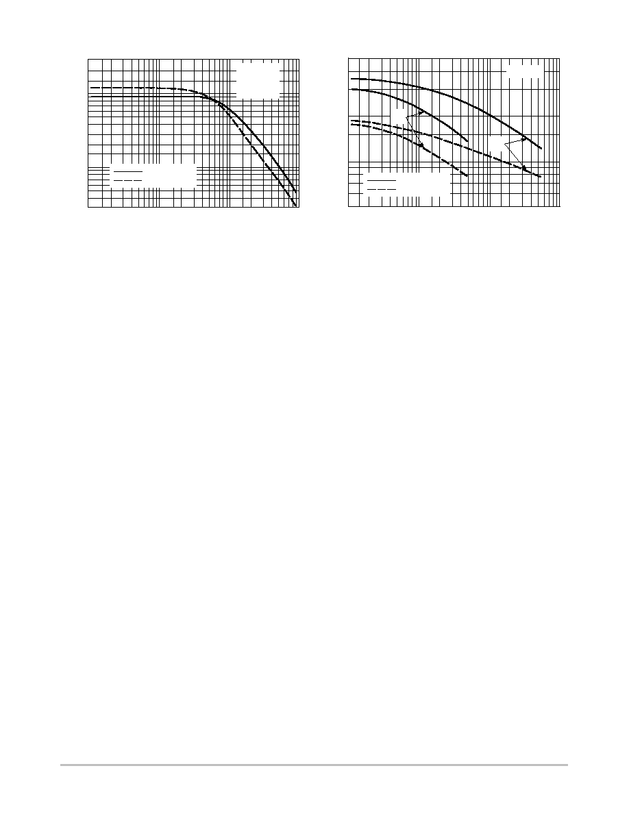
There are two limitations on the power handling ability of
a transistor: average junction temperature and second
breakdown. Safe operating area curves indicate I
C
≠ V
CE
limits of the transistor that must be observed for reliable
operation; i.e., the transistor must not be subjected to greater
dissipation than the curves indicate.
The data of Figures 5, 6, and 7 is based on T
J(pk)
= 200
_C;
T
C
is variable depending on conditions. Second breakdown
pulse limits are valid for duty cycles to 10% provided T
J(pk)
v 200_C; T
J(pk)
may be calculated from the data in Figure
4. At high case temperatures, thermal limitations will reduce
the power that can be handled to values less than the
limitations imposed by second breakdown.
2N6052
http://onsemi.com
4
500
0.1
Figure 7. Small≠Signal Current Gain
V
R
, REVERSE VOLTAGE (VOLTS)
50
1.0
2.0
100
5.0
0.2
0.5
C, CAP
ACIT
ANCE (pF)
300
100
70
T
J
= 25
∞
C
C
ib
200
C
ob
3000
1.0
Figure 8. Capacitance
f, FREQUENCY (kHz)
30
2.0
5.0
20
50
1000
100
10
10
20
50
h fe
, SMALL-SIGNAL
CURRENT
GAIN
2000
1000
500
200
100
50
200
500
2N6052
2N6058/2N6059
T
C
= 25
∞
C
V
CE
= 3.0 V
I
C
= 5.0 A
2N6052
2N6058/2N6059

2N6052
http://onsemi.com
5
V CE
, COLLECT
OR-EMITTER VOL
T
AGE (VOL
TS)
V CE
, COLLECT
OR-EMITTER VOL
T
AGE (VOL
TS)
20,000
0.2
Figure 9. DC Current Gain
I
C
, COLLECTOR CURRENT (AMP)
200
0.3
0.5
1.0
2.0
20
h FE
, DC CURRENT
GAIN
10
PNP
2N6052
NPN
2N6058, 2N6059
Figure 10. Collector Saturation Region
3.0
0.5
I
B
, BASE CURRENT (mA)
1.0
1.0
2.0
10
50
1.8
I
C
= 3.0 A
T
J
= 25
∞
C
6.0 A
2.2
2.6
5.0
3.0
0.2
I
C
, COLLECTOR CURRENT (AMP)
0.3
0.5
1.0
3.0
20
2.5
2.0
1.5
1.0
0.5
T
J
= 25
∞
C
V
BE(sat)
@ I
C
/I
B
= 250
V
CE(sat)
@ I
C
/I
B
= 250
V
,
VOL
T
AGE (VOL
TS)
Figure 11. "On" Voltages
V
BE
@ V
CE
= 3.0 V
2.0
10,000
T
J
= 150
∞
C
25
∞
C
-55
∞
C
20
I
C
, COLLECTOR CURRENT (AMP)
h FE
, DC CURRENT
GAIN
V
CE
= 3.0 V
T
J
= 150
∞
C
25
∞
C
-55
∞
C
1.4
9.0 A
I
B
, BASE CURRENT (mA)
T
J
= 25
∞
C
I
C
, COLLECTOR CURRENT (AMP)
T
J
= 25
∞
C
V
,
VOL
T
AGE (VOL
TS)
V
BE
@ V
CE
= 3.0 V
5000
3000
2000
1000
500
300
3.0
5.0
V
CE
= 3.0 V
40,000
0.2
400
0.3
0.5
1.0
2.0
20
10
20,000
10,000
6,000
4,000
2,000
1,000
600
3.0
5.0
3.0
3.0
1.0
1.8
2.2
2.6
1.4
10
5.0
3.0
0.2 0.3
0.5
1.0
3.0
20
2.5
2.0
1.5
1.0
0.5
2.0
10
5.0
30
12 A
I
C
= 3.0 A
6.0 A
9.0 A
12 A
0.5
1.0
2.0
10
50
5.0
20
3.0
30
V
BE(sat)
@ I
C
/I
B
= 250
V
CE(sat)
@ I
C
/I
B
= 250